Classification of Industrial Additive Manufacturing (AM)

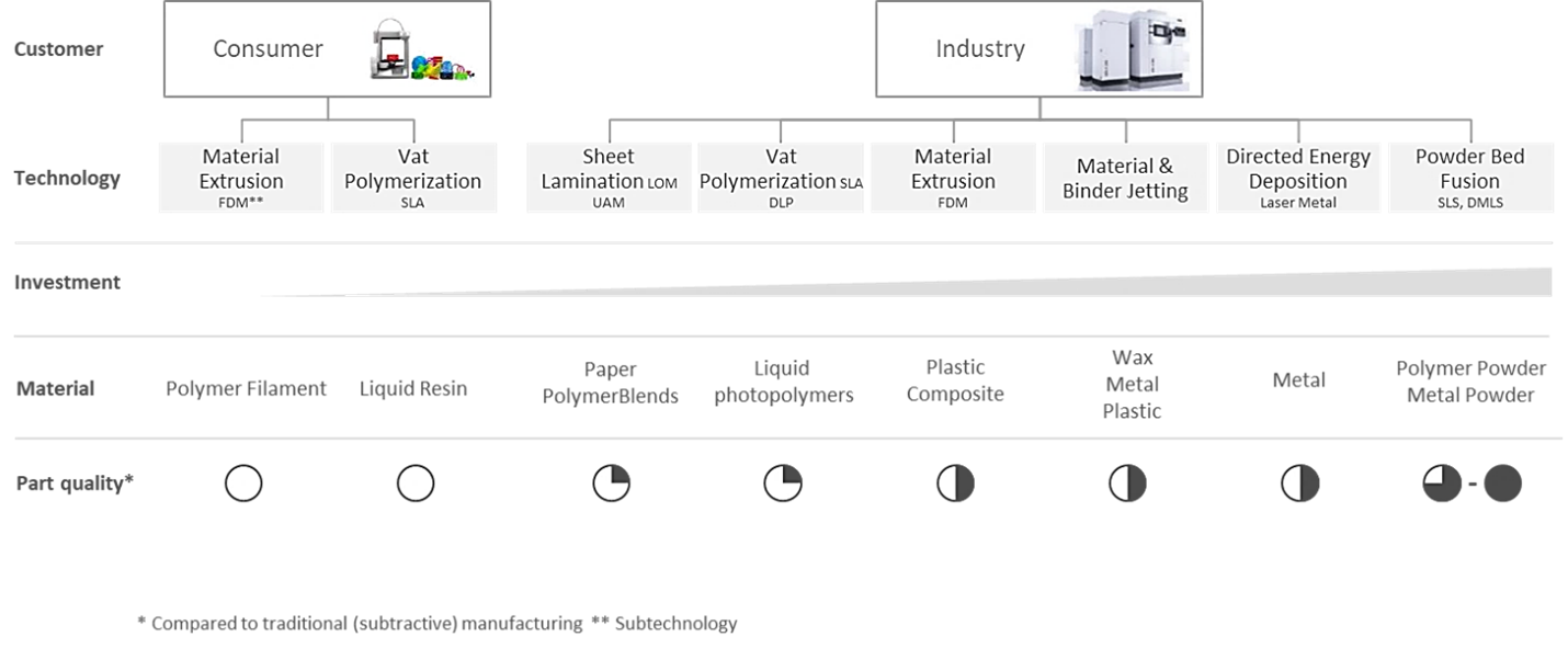
Classification based on the overall Landscape of Additive Manufacturing

The AM is broadly classified into 2 categories:

  • Technology
  • Materials


Figure (1): Classification based on the overall Landscape of Additive Manufacturing (Image Courtesy oftoof EOS GmbH)


Technology

Technological Classification of Additive Manufacturing:

Today, Additive Manufacturing (AM) is not only available for industry grade applications but also for hobby printing thanks to learning- grade tabletop printing machines. Broadly there are 7 categories of AM processes worldwide while new techniques and processes are being introduced due to continuous emergence and expansion of this industry.

  • VAT Photo – Polymerisation
  • Material Jetting
  • Binder Jetting
  • Material Extrusion
  • Powder Bed Fusion
  • Sheet Lamination
  • Direct Energy Deposition


VAT Photo – Polymerisation

VAT Photo – Polymerisation is an additive manufacturing process where a liquid photopolymer resin is selectively cured by a light source to build up a part layer by layer. The term “VAT” refers to the vat or container that holds the liquid resin during the printing process.

The VAT photo – polymerisation is further categorised into the following:

  • Stereolithography (SLA)
  • Digital Light Processing (DLP)
  • Hybrid Photosynthesis Technology (HPS) [SLA + DLP]
  • Liquid Crystal Display (LCD)
  • Lubricant Sublayer Photo – Curing (LSPc)
  • Programmable Photo Polymerisation (P3)
  • Continuous Digital Light Manufacturing (CDLM)
  • Continuous Liquid Interface Production (CLIP)


Material Jetting (MJ)

Material Jetting is an additive manufacturing process that works similarly to inkjet printing but instead of jetting ink, it deposits droplets of build material layer by layer to create a 3D object. Each layer is immediately cured or solidified using ultraviolet (UV) light, allowing for the creation of highly detailed and accurate parts.

The material jetting (MJ) is further categorized as follows:

  • Material Jet Printing (MJP)
  • Liquid Metal Jetting (LMJ)
  • Polyjet (PJ)


Binder Jetting (BJ)

Binder Jetting is an additive manufacturing process that uses a liquid binding agent to selectively bind powder particles together to form a solid part. The process builds parts layer by layer, like other AM technologies, but it stands out for its ability to handle a wide range of materials and its relatively low cost.

The Binder Jetting (BJ) process is further categorized as:

  1. Single Pass Jetting (SPJ)


Material Extrusion (ME)

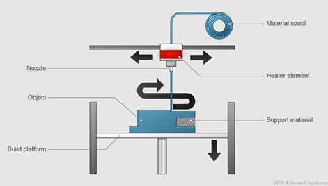
Material Extrusion is an additive manufacturing process where a thermoplastic material is heated until it becomes semi-liquid and is then extruded through a nozzle to build up an object layer by layer. The extruded material solidifies and bonds with the previous layer, gradually forming the desired 3D shape.


Figure (2): Material Extrusion Process

The Material extrusion is further categorized into following:

  • Fused Deposition Modelling (FDM)
  • Fused Filament Fabrication (FFF)
  • High Speed Extrusion (HSE)
  • Independent Dual Extruder (IDEX)
  • Cast in Motion (CIM)
  • Atomic Diffusion Additive Manufacturing (ADAM)


Powder Bed Fusion (PBF)

Powder Bed Fusion is an additive manufacturing process where a heat source, typically a laser or electron beam, selectively fuses powdered material layer by layer to build a part. The process occurs in a controlled environment to ensure high precision and material properties.

The Powder Bed Fusion is further categorized into following:

  • Laser Powder Bed Fusion (LPBF) further also known as:
    • Selective Laser Sintering (SLS)
    • Cold Metal Fusion (CMF)
    • Quantum Laser Sintering (QLS)
    • High Speed Sintering (HSS)
    • Direct Metal Laser Solidification (DMLS)
    • Selective Laser Melting (SLM)
    • Direct Metal Laser Melting (DMLM)
    • Hybrid Laser Powder Bed Fusion with CNC (HLPBF)


  • Multi Jet Fusion (MJF)
  • Selective Absorption Fusion (SAF)
  • Electron Beam Melting (EBM)
  • Mold Jet Technology (MJT)


Sheet Lamination

Sheet Lamination, also known as Laminated Object Manufacturing (LOM), involves layering sheets of material and bonding them together to form a solid part. Each sheet is precisely cut to match the cross-sectional shape of the part at a particular layer. The layers are bonded using adhesives, heat, or pressure, creating a cohesive structure.


Direct Energy Deposition (DED)

Direct Energy Deposition is an additive manufacturing process that uses focused thermal energy, such as a laser, electron beam, or plasma arc, to fuse materials by melting them as they are being deposited. This technology can work with various materials, including metals, ceramics, and composites, making it highly versatile for different industrial applications.

The Direct Energy Deposition (DED) is further categorized as follows:

  • Laser Direct Energy Deposition (LDED)
  • Hybrid Laser Direct Energy Deposition with CNC (HLDED)
  • Rapid Plasma Deposition (RPD)
  • Wire Arc Additive Manufacturing (WAAM)

Materials

AM classifications based on Raw Material Form/Shape and Feed:


Extrusion Based Additive Manufacturing

Extrusion-based additive manufacturing is a process where a thermoplastic material is heated until it becomes semi-liquid and is then extruded through a nozzle to build up an object layer by layer. The extruded material solidifies and bonds with the previous layer, gradually forming the desired 3D shape.


Resin Based Additive Manufacturing

Resin-based additive manufacturing involves the use of liquid photopolymer resins that are selectively cured by a light source to form solid layers. These layers are built up sequentially to create a complete 3D object. The process is known for its high resolution and ability to produce intricate details and smooth surface finishes.


Powder Based Additive Manufacturing

Powder-based additive manufacturing involves spreading a layer of powdered material, which is selectively fused by an energy source to form a solid layer. The process repeats layer by layer until the entire part is built. The unfused powder supports the part during the build, eliminating the need for additional support structures.


Sheet Based Additive Manufacturing

Sheet-based additive manufacturing builds objects by stacking, bonding, and cutting sheets of material. Each sheet is cut to the desired shape using a laser or mechanical cutter and bonded to the previous layer to form the final 3D part. This method can utilize a variety of materials, including paper, plastic, and metal.


Stay tuned to our Blog series to get further information on the above technologies in detail.

A Unique Revolution: Manufacturing Tire Sipes with EOS DMLS and the M290 System

Overview

In the tire industry, precision and efficiency are paramount when producing high-quality tires that perform optimally on the road. With increasing pressure to innovate while maintaining cost-effectiveness, tire manufacturers are turning to 3D printing as a transformative solution. The combination of EOS Direct Metal Laser Solidification (DMLS) technology and the EOS M290 system is revolutionizing how tire mold sipes are produced, offering improved performance, reduced cycle times, and significant cost savings.


The EOS DMLS Process: Advancing Tire Mold Production

EOS DMLS is a state-of-the-art metal 3D printing technology that uses a high-powered laser to fuse fine metal powders into solid metal parts, layer by layer, directly from a 3D CAD model. This additive manufacturing process allows for the creation of complex geometries that traditional methods, such as machining or casting, cannot achieve. In the context of tire mold sipes, this means manufacturers can produce intricate tread patterns and molds with greater precision, speed, and efficiency.

The EOS M290 system, a highly versatile and precise 3D printing platform, is specifically designed for industrial applications like tire mold production. Its capabilities make it the ideal system for manufacturing tire mold sipes with the accuracy and reliability required to meet industry standards.


Why EOS DMLS and the M290 System Are Perfect for Tire Mold Sipes

  • Complex Mold Designs Made Simple

    Traditional tire mold manufacturing methods can struggle to create intricate tread patterns due to the limitations of machining and casting. With the EOS DMLS process, the M290 system can print highly detailed and complex shapes that are impossible to achieve with conventional methods. This capability is crucial for producing advanced tire sipes—the patterns that play a critical role in improving tire performance, such as traction, durability, and handling.

  • Precision and Customization

    The ability to create custom molds with high precision is one of the key benefits of 3D printing. The EOS M290 system enables tire manufacturers to experiment with different tread designs, optimizing them for various driving conditions. Whether it’s for high-performance tires or eco-friendly models, the M290 system ensures that every mold is crafted to exact specifications, delivering optimal tire performance and consistency.

  • Faster Production and Shorter Lead Times

    Traditional tooling for tire molds can take weeks to manufacture, with long lead times that delay production schedules. The EOS M290 system drastically reduces these lead times by enabling rapid prototyping and direct production of the final mold. Once the design is ready, the mold can be produced in a matter of days, not weeks. This faster production capability allows tire manufacturers to quickly respond to market demands and reduce time-to-market for new tire models.

  • Cost-Efficiency

    Traditional mold-making processes often result in material waste, as large portions of the mold material are machined away. With 3D printing, the EOS M290 system uses only the material needed to build the mold, minimizing waste and lowering production costs. This cost-efficient approach is particularly valuable for tire manufacturers who need to balance precision and performance with cost-effectiveness.

  • Improved Tool Durability

    The EOS DMLS process produces molds with enhanced durability compared to traditional methods. With precise control over the material properties, tire manufacturers can produce molds that are not only strong but also resistant to wear and tear over time. The result is longer-lasting tools that require less maintenance, ensuring that tire production remains consistent and high-quality.


EOS M290: The Ideal System for Tire Mold Sipes Production

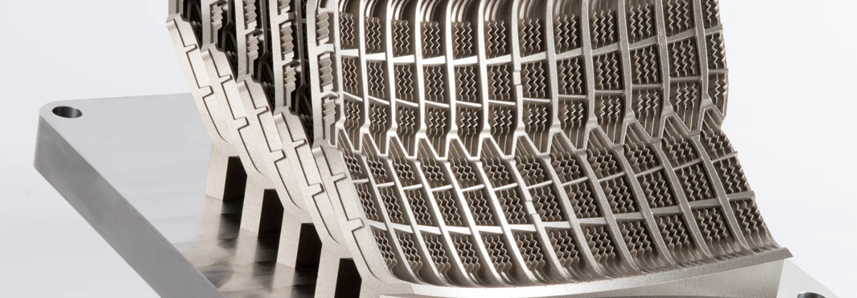
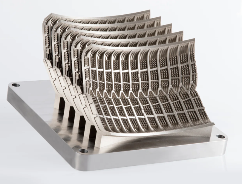
The EOS M290 system is specifically designed to meet the demands of industrial 3D printing, making it the perfect choice for tire mold production. This mid-size 3D printer offers high precision and a broad range of metal materials, including Maraging Steel, Tool Steel, and Stainless Steel, which are ideal for creating durable and high-performance tire molds.

Fig. (1): Build plate with tire mould sipes from EOS M290 system|(Image Courtesy: EOS website)


With the EOS M290 system, tire manufacturers can harness the full potential of DMLS technology to produce molds that are more precise, more durable, and more efficient than those made with traditional methods. The system’s high productivity and scalability make it suitable for both prototype and large-scale production, allowing manufacturers to streamline their processes and increase output.


The Impact of EOS DMLS on Tire Manufacturing

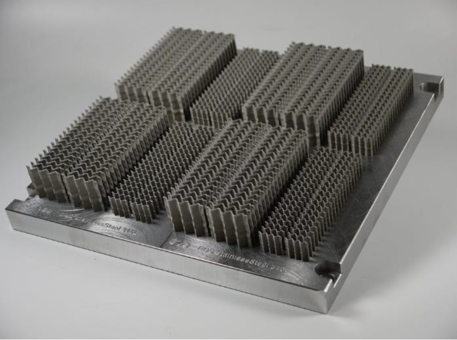
The ability to produce highly detailed tire molds with complex geometries using EOS DMLS technology and the M290 system has had a profound impact on the tire industry. By reducing production times, lowering costs, and increasing precision, tire manufacturers are now able to meet the ever-growing demands for performance, durability, and customization.

Additionally, the flexibility offered by 3D printing allows manufacturers to produce molds in small batches, experiment with new tread patterns, and rapidly prototype new tire designs—all without the need for expensive tooling changes or long production delays.

Fig. (2): Marigo Tire Mold Insert printed using EOS DMLS system|(Image Courtesy: EOS website)


Conclusion

The tire industry is experiencing a shift towards more efficient, cost-effective, and innovative production methods, and EOS DMLS technology with the M290 system is at the forefront of this transformation. By enabling the creation of high-precision tire mold sipes with faster lead times, reduced costs, and improved durability, the M290 system is revolutionizing the way tire molds are manufactured.

For tire manufacturers looking to stay ahead of the curve and enhance their production processes, embracing 3D printing with EOS DMLS technology is essential. The future of tire mold production is here, and it’s powered by the EOS M290 system.

Fig. (3): EOS M290 system suitable for mould manufacturing|(Image Courtesy: EOS website)

Innovating Design in the Space Industry with 3DEXPERIENCE CATIA

The space industry is at the forefront of technological advancement, with its unique challenges demanding cutting-edge tools for design and engineering. From satellites and spacecraft to rockets and space stations, the need for precision, collaboration, and innovation is unparalleled. This is where 3DEXPERIENCE CATIA shines, empowering organizations to transform their ideas into reality while overcoming the complexities of space exploration.


Addressing the Unique Challenges of Space Design

  • Extreme Precision: Components must withstand the harsh conditions of space, including extreme temperatures, vacuum environments, and radiation.
  • Weight Optimization: Every gram counts, as launch costs are heavily influenced by payload weight.
  • Complex Systems Integration: Spacecraft involve intricate systems that need seamless integration, from propulsion and avionics to communication and life support.
  • Global Collaboration: Teams across the globe often contribute to a single mission, necessitating streamlined communication and data sharing.

Advanced Capabilities for Space Design

  • Parametric and Generative Design: CATIA’s parametric modelling enables engineers to create highly detailed and adaptable designs. Generative design capabilities further allow teams to explore innovative structures optimized for weight and strength, which is essential for space applications.
  • Multiphysics Simulation: Space components must endure extreme stresses. CATIA’s integration with simulation tools allows for detailed analysis of thermal, structural, and aerodynamic properties, ensuring reliability under harsh conditions.
  • Virtual Twin Technology: The Virtual Twin Experience on the 3DEXPERIENCE platform allows designers to create a digital replica of a spacecraft, enabling real-time analysis, testing, and optimization before physical prototypes are built.

Enhancing Collaboration in Space Projects

The 3DEXPERIENCE platform facilitates seamless collaboration across teams and disciplines. With a centralized data repository, stakeholders can access the latest design iterations, provide feedback, and ensure alignment throughout the development process.

  • Real-Time Collaboration: Engineers, scientists, and project managers can work on the same model simultaneously, regardless of location.
  • Traceability and Compliance: The platform ensures that every design decision is documented, aiding in compliance with aerospace regulations.
  • Stakeholder Engagement: Visual and immersive tools help non-technical stakeholders understand and contribute to design decisions.

Success Stories in Space Design

Organizations leveraging 3DEXPERIENCE CATIA have achieved remarkable milestones in space exploration. From designing lightweight satellite structures to developing reusable rocket components, CATIA has proven its versatility and reliability in driving innovation.


Sustainability in Space Design

Sustainability is becoming a critical concern in the space industry. With CATIA, teams can:

  • Optimize designs to minimize material waste.
  • Explore the use of eco-friendly materials.
  • Improve energy efficiency in manufacturing and operations.

Conclusion

The space industry’s demands for innovation, precision, and collaboration are met with unparalleled effectiveness by 3DEXPERIENCE CATIA. By enabling teams to design, simulate, and optimize within a unified platform, CATIA is not just a tool but a catalyst for the next frontier of exploration. As we continue to push the boundaries of what is possible, CATIA will remain an indispensable partner in crafting the future of space exploration.

Enhancing Semiconductor Design with EDA Tools and Solutions

Overview

The semiconductor industry demands cutting-edge tools to address the complexities of modern chip design. As a trusted partner, EDS Technologies supports the adoption of Synopsys’ advanced Electronics Design Automation (EDA) solutions, enabling efficient development of Application Specific Integrated Circuits (ASICs) and Systems on Chip (SoCs). These solutions cater to the growing need for high-performance, low-power designs that power applications across industries, from consumer electronics to aerospace. 


Importance of Synopsys EDA tools in Chip design 

They minimize the risk and reduces the trial-and-error costs. The chip cannot be altered once it is manufactured. Their designs are extremely complex and involves high development and R&D cost. The tools can diagnose complex physical problems as quantitative models, simulate circuit process in virtual software, and reproducing multiple effects in the chip development cycle. One of the highlights of Synopsys EDA suite is to simulate and optimize the PPA (Power, Performance and Area), which solves the multiple objectives and problems and reduces the cost of trial and error. 


Chip Designing Process 

The chip design process is divided into front-end design and back-end design.

Front End Design: 

Front end which is known as logic design involves the functional design of the chip. From defining the chip architecture to generating the netlist is the front-end design, which also involves a functional verification to verify the circuit functions and logic.  

  • Design: RTL creation can be performed using the Euclide and Synopsys RTL Architect is a predictive RTL design solution that provides early predictions of the impact of the RTL changes on your PPA.  
  • Lint, CDC (Clock Domain Crossing) and RDC (Reset Domain Crossing) : RTL errors are very crucial in SoC design which may lead to design failure or even re-spins of the chip. Synopsys SpyGlass offers early RTL Analysis during the RTL design phase to avoid linting, CDC and RDC errors.
  • Simulation (Functional Verification) : Synopsys VCS tool is a widely popular tool for the formal verification to simulate the RTL design meeting its design specifications. VCS is capable of mixed language simulation, supports UVM, OVM VMM methodologies, and Verification IPs. All the gate level simulations and power simulations can be performed in VCS. 
  • DFT – Design for Testability : DFT is a testing technique in IC design during the manufacturing process by implementing additional design features to ensure the designed circuit is free from any kind of manufacturing defects. Synopsys TestMAX DFT is a comprehensive tool which supports all essential DFT such as boundary scan, scan chains, core wrapping, test points and compression. They can be implemented using TestMAX manager for early validation of the corresponding RTL or with Synopsys Synthesis tools for generating the netlists. 
  • Synthesis:  Design compiler and Synplify are the two Synthesis solutions from Synopsys for the IC designs and FPGA designs respectively, which are widely popular across the industry. Design compiler supports mixed language placement aware synthesis, optimization of multi voltage, low power synthesis, placement aware physical synthesis and multi-threading. Synplify has faster runtime, performance, area optimization for cost and power reduction, multi–FPGA Vendor support, incremental and team design capabilities for faster FPGA designs. 


Back End Design 

Back-end which is also known as Physical design involves process related design. The major activities are placing and routing the millions of transistors on a chip, to optimize the Power, Performance and Area. 

  • Physical Design: Physical Design comprises of Floor Planning, Place and Route, Power planning, Low power analysis and Power estimation. All these can be achieved by using Synopsys IC Compiler. 
  • Physical Verification: Correctness and reliability of the physical layout of the ICs are verified through a critical process of Physical Verification. The process involves verifying the design against a set of design rules to ensure that the final product functions are intended. Synopsys IC Validator can perform the Design Rule Checks (DRC), Layout versus Schematic (LVS), Electrical Route Check (ERC), GDS comparison, Netlist-to-Netlist verification, Layout vs Layout and Antenna Checks. 
  • Sign-off: Synopsys is a leading solution provider in the design sign-off innovations, which addresses the challenges of complex design, scale and new requirements for chip design on advanced processor nodes. The sign-off is done with Synopsys IC Compiler II. 
  • Synopsys IP Solutions: Synopsys Silicon IPs are the most popular and has a wide portfolio of solutions with proven results across the industry. Logic Libraries, Embedded Memories, Interface IPs, Embedded Processors and Subsystems fall under the IP portfolio. The IPs are optimized for a wide range of market segments like Internet of Things, Automotive, Artificial Intelligence, 5G Mobile and Data Center. 

Synopsys Manufacturing Solutions

Synopsys is a market leader in offering the Silicon Manufacturing and Silicon Life cycle management solution. It includes TCAD (Technology Computer Aided Design), Mask Synthesis and Manufacturing Analytics. The Synopsys manufacturing solutions are customized for expertise in IC design, mask synthesis, process modelling, on-chip test and monitoring techniques and cloud-based analytics. 


How Foundries are Benefiting with Synopsys  

Synopsys is collaborating with Intel for developing interface and Foundation IPs for Intel Foundry’s latest process for their high-power efficiency System-on-Chips. They have been collaborating for decades to accelerate the design productivity. Intel and Synopsys together are driving the next gen system innovations for a wide range of applications like High Performance Computing (HPCs), Automotive, Mobile and Aerospace.  

Taiwan Semiconductor Manufacturing Company Limited, which contributes more than 50% of the market share in chip manufacturing is also collaborating with Synopsys by using their silicon IPs, EDA Tools and multi-die system design flow and Photonic IC design flows for their advanced process technologies. This collaboration of over 20 years have helped them deliver high quality interface IPs and foundation IPs for their process technology from 180nm to 3nm for applications like HPCs, AI, Automotive and Mobile. 


EDS Technologies: Your Partner in Semiconductor Design

EDS Technologies is committed to enabling semiconductor companies to harness the full potential of Synopsys EDA solutions. Our expertise ensures seamless adoption of these tools, helping customers achieve their project goals. Together with Synopsys, we aim to empower businesses with state-of-the-art technologies that drive innovation across industries. 

Game Changing EOS Systems for Lifestyle and Consumer Goods Industry: Eyewear Applications

Every person’s face is as unique as their personality, making custom eyewear not just a luxury but a necessity for optimal comfort and functionality. Traditional methods of manufacturing glasses frames are labor-intensive and costly, especially when tailored to individual needs. However, industrial 3D printing, particularly with EOS systems, has revolutionized this process, offering unmatched customization, efficiency, and sustainability.


The Power of EOS Technology in Eyewear Manufacturing

EOS additive manufacturing systems enable the production of both metal and plastic glass frames that meet the highest demands for design, functionality, and aesthetics. By combining cutting-edge technology with innovative materials like PA 2200, eyewear manufacturers can deliver frames that are not only lightweight and robust but also tailored to the unique facial features of each customer.

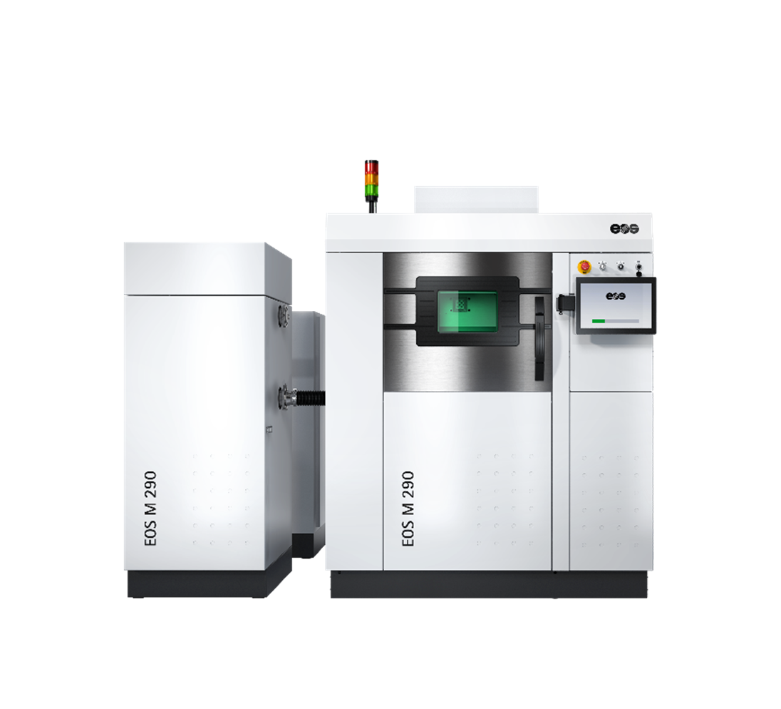
Fig.1: EOS system configuration for Eyewear production on demand


Key Advantages of EOS 3D Printing for Eyewear

  • Virtually Limitless Customization: Glass frames can be designed to fit the exact contours of a customer’s face using 3D scanning technology.
  • Enhanced Comfort: Lightweight and stable designs ensure maximum wearability.
  • Sustainability: Reduced material waste and the ability to reuse leftover material make the process eco-friendly.
  • Rapid Prototyping and Production: Quick turnaround times enable faster time-to-market and the ability to respond to customer demands swiftly.
  • Cost-Efficiency: Additive manufacturing eliminates the need for minimum order quantities, allowing for the economical production of small batches or single units.

Success Story: 3x More Sustainable 3D Printed Eyewear by You Mawo

The innovative start-up You Mawo exemplifies the transformative potential of EOS 3D printing technology in eyewear. By leveraging the EOS P 396 system and PA 2200 material, You Mawo produces glasses frames that are:

  • 30% Lighter than Acetate: The reduced weight enhances comfort without compromising durability.
  • Tailored to Individual Needs: Frames are based on 3D scans of customers’ faces, ensuring a perfect fit.
  • Environmentally Friendly: Additive manufacturing minimizes overproduction and shortens delivery paths, reducing the carbon footprint.


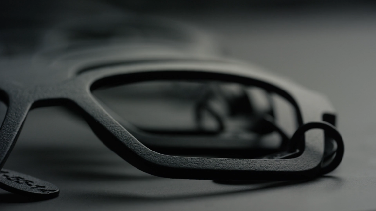
Fig. 2: Production of Customized and Personalized Eyewear using EOS SLS Process


The BRAGi Eyewear Revolution

Nanjing BRAGi Optical Technology Co., Ltd., has embraced EOS additive manufacturing for its business model. Using the FORMIGA P 110 Velocis system and PA 2200 material, BRAGi has created a streamlined process that includes:

  • Scan-to-Print Workflow: Customers’ facial data is captured via 3D scanning, enabling precise customization.
  • High-Quality Finishes: The material’s purity and surface quality allow for seamless post-processing and vibrant coloring.
  • Hypoallergenic and Durable Frames: The glasses are not only lightweight and robust but also hypoallergenic, making them suitable for sensitive skin.


In just a few months, BRAGi produced over 30,000 custom glasses frames, expanding its market across Asia and receiving inquiries from Europe. This success underscores the scalability and global appeal of additive manufacturing in the eyewear industry.

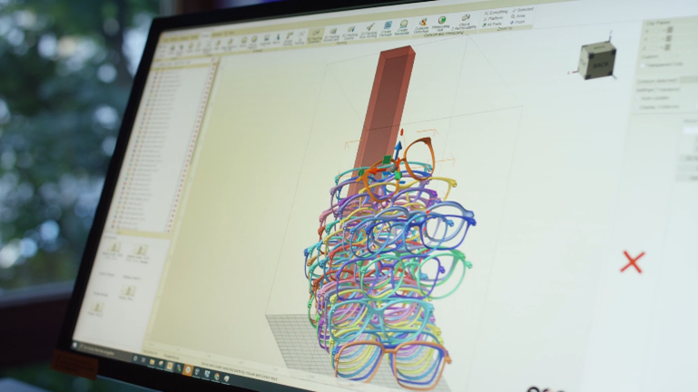
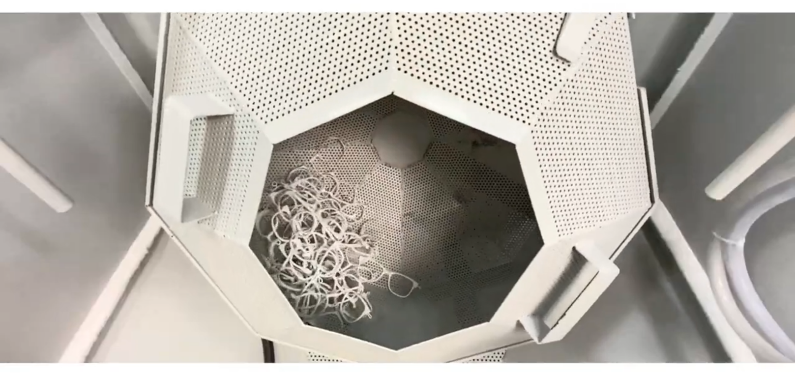
Fig. 3: Scaled Finishing process for Production of Eyewear

The Strategic Advantage: P3 Next System for Eyewear Manufacturing

For eyewear manufacturers looking to scale their operations while maintaining precision and quality, the P3 Next system offers an unmatched commercial advantage. Its cutting-edge capabilities are tailored to meet the high demands of the eyewear industry, delivering both cost efficiency and superior performance.

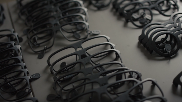
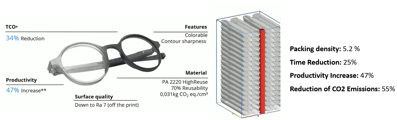
Fig. 4: Improved throughput of efficient EOS P3 Next for Eyewear Application


Key Advantages of the P3 Next System

  • Enhanced Productivity: Optimized workflow and innovative software boost machine productivity by 50% while reducing costs by 30%.
  • Maximized Machine Availability: Achieve up to 90% machine availability with double material efficiency and an impressive 80% reusability rate.
  • Advanced Software Solutions: Efficiently manage data preparation, production, and analytics for streamlined operations.
  • Innovative Peripherals: Simplify workflows with state-of-the-art peripherals for part unpacking, finishing, material sieving, and mixing.
  • Scalable and Cost-Effective: Enable scalable production with a minimal footprint, perfect for growing businesses.
  • Precision-Driven Quality: Deliver consistent, high-quality results tailored to every application.
  • Quick Time-to-Market: Leverage optimized and proven parameter sets to accelerate production timelines.
  • Customizable Settings: Enhance both quality and performance with adjustable settings designed for specific needs.


Reinventing the Automotive Supply Chain with the Digital Experience Platform

Increased product complexity, global sourcing & disruptions, uncertainty, sustainability and regulatory pressures, consumer demand shifts, and cost pressures are some of the significant challenges that the automotive supply chain is facing today. These challenges demand a reinvention to remain resilient, efficient, and responsive to the evolving market. Connecting every stakeholder in the ecosystem can improve collaboration, streamline processes, and enhance product development to rapidly changing market conditions.


Digital Transformation: Catalyst to Reinvent Automotive Supply Chain

Digital transformation is no longer just a trend but a fundamental shift in how automotive industries operate and evolve. For the automotive supply chain, digital transformation offers an unprecedented opportunity to enhance efficiency, responsiveness, and resilience. By integrating advanced technologies, the automotive industry can break down silos, enhance real-time data access, and accelerate decision-making processes.

The 3DEXPERIENCE platform by Dassault Systèmes provides a suite of integrated tools that enable seamless collaboration between Automotive Original Equipment Manufacturers (OEMs) and their suppliers. This digital platform allows both teams to collaborate more efficiently, manage data, and enhance innovation throughout the product lifecycle.


Here’s a breakdown of how the 3DEXPERIENCE Platform can revolutionize the automotive supply chain

  • Integrated Digital Collaboration Hub: Cross-Disciplinary Collaboration within the company & supplier engagement
  • Supplier-Integrated Design & Development: Co-Design Capabilities & Concurrent Engineering
  • Real-Time Visibility and Traceability: Digital thread with real time updates
  • Collaborative Supply Chain Management
  • Collaborative product development with comphrensive & transparent change management process
  • Advanced Simulation and Testing
  • Supplier Performance Management
  • Cloud-Based Collaboration for Global Teams
  • Sustainability and Environmental Impact assessment solutions


3DEXPERIENCE Solution Landscape for Automotive Supply Chain


Overall, the 3DEXPERIENCE platform empowers OEMs and their suppliers to work together more efficiently, transparently, and innovatively across the entire automotive product lifecycle. By providing a collaborative digital environment that integrates design, engineering, manufacturing, and supply chain management, 3DEXPERIENCE enhances the ability of OEMs and suppliers to align on goals, resolve issues faster, and accelerate time-to-market. From real-time data access and collaborative design to supplier performance management and advanced simulations, this platform is a game-changer for the automotive industry, driving greater innovation and operational efficiency.

To get more information & insights on how the 3DEXPERIENCE Platform drives business transformation in the automotive industry, please reach out to us at marketing@edstechnologies.com

Subscribe to our newsletter

Get all the latest information on Events, Sales and Offers.